Sophia Magazine vol.4 / WINTER 2016
12/32
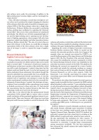
side surfaces more easily, the percentage of gallium in the light-emitting layer becomes higher, and the wavelength be-comes shorter.”Thus, with these techniques, crystals that emit light in vari-ous colors can be produced by simply changing the diameter of the columns which also makes it possible to integrate nano-column LEDs of the three primary colors into a single chip. Furthermore, Professor Kishino has succeeded in producing surface-emitting laser oscillation by exploiting the “photonic crystal effect” that occurs when nanocolumns are positioned periodically. The effective use of freely manipulated light col-ors and the light-emitting area is opening up new develop-ment of lighting apparatuses, ultra-compact full-color laser projectors, retinal scan displays and other innovative devices. Professor Kishino details that “The sizes of current chips are about 200×200μm2. In the future, we would like to integrate nanocolumn LEDs of the three primary colors into a single chip of 10×10μm2 in order to expand the range of applica-tions.”Professor Kishino says that this nanocolumn breakthrough is actually a by-product of a failed endeavor that can be traced back to around 1996: “I instructed a fourth-year student at my laboratory at that time to produce a flat nitride film, which was still in early development. I waited a long time, but this student could not finish the task. Up to the last moment, just before graduation thesis submission, this student thought the outcome submitted was unsuccessful, but it was actually ran-domly and spontaneously formed nanocolumns. It was this student’s lack of experience and attempt to create the film under unanticipated conditions that led to this successful de-velopment of nanocolumns. I praised this developer of nano-columns. Even in scientific circles, nanocolumns were treated as freakish occurrences in those early days. If I had rejected the nanocolumns that the student formed at that time, this technology would never have been developed.”After that, it was observed that the spontaneously formed nanocolumn LEDs emitted light in various colors as jewels would, and photos of this generated significant interest in aca-demic circles. There was, however, still a long way to go from that point until it became possible to control the diameter of the columns and produce crystals that could emit the desired color. That control became possible by adopting a titanium mask, ac-cording to the paper explaining this, published in 2008. Regarding the extent of Sophia University’s involvement, Professor Kishino mentions that “While we carried out the research, the university provided us with a lot of support. For example, when our research was selected by CREST, a re-search-funding program of the Japan Science and Technology Agency (JST), the Vice President of the university helped se-cure a space for installing the necessary equipment. In 2008, the Nanotechnology Research Center was established at the university to promote research in this field. This platform for facilitating the research was supported by a team of profes-sors inside and outside the university working on a project that received Grant-in-Aid for Scientific Research (Specially Promoted Research) as well as other projects. Under this framework, I am currently supervising two project teams researching nanocrystal effects and developing nanocrystal-based devices.”The professor also relates that Sophia University’s generous support made it possible for him to research the MBE method ahead of parties in other countries. “I was conducting research on red semiconductor lasers using gallium indium phosphide (GaInP) when I was appointed at Sophia University in 1984. During that period, Professor Robert Deiters, S.J., who was then the head of the Department of Electrical and Electronics Engineering (currently the Department of Engineering and Applied Sciences), supported my research by persuading the department to allow me to use part of the research budget for large-scale equipment. That is how I was able to install a cutting-edge MBE system. I will always be very grateful for his support.”Professor Kishino’s research ultimately produced remark-able results because, although many researchers of nitrides at that time were studying crystal growth using the Metal Organic Chemical Vapor Deposition (MOCVD) method, the university’s support gave him a head start in working on the MBE method, an approach better suited for basic research. He also appreciates this institution for other reasons: “I like the name ‘Sophia University’ which is easy for overseas researchers to remember. It greatly helps communication among researchers worldwide. The fact that missionaries have advanced the school’s mission also makes Sophia Uni-versity distinctive.”Research Backed by Sophia University SupportMicro-EL MeasurementNear eld EL emission image of self-assembled nanocolumn LEDs20umResolution2μm12Research
元のページ