Sophia Magazine vol.4 / WINTER 2016
11/32
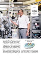
fine nanoscale needle shape. There is high expectation that this technology can be used to make LEDs that are highly ef-ficient at emitting light, even red light, a long wavelength.”The method used to produce this semiconductor is as fol-lows: First, a titanium nano-hole mask is formed on a GaN film prepared on a sapphire substrate. Next, molecular beams of gallium and indium irradiate the mask surface using the Molecular Beam Epitaxy (MBE) method while nitrogen is supplied. This method makes it possible to grow column-shaped nanocrystals (nanocolumns) only at the mask open-ing on the GaN film. “When this process is performed, not only the top portion, but also the side surfaces of the nano-columns are irradiated by the molecular beams. Only gallium diffuses on the side surfaces to the top and is absorbed at the top portion, which increases the amount of gallium incorpo-rated into the crystal at the top. Therefore, the ratio of gallium in the InGaN light-emitting layer formed on the top portion increases. When the diameter of the periodically positioned adjacent nanocolumns is smaller, the beam shadowing effect becomes weaker. As a result, molecular beams can strike the CHRONICLESOF RESEARCHERS AT SOPHIA KATSUMIKISHINOProfessorDepartment of Engineeringand Applied SciencesFaculty of Science andTechnology#07Three primary colors integratednanocolumn LEDsInGaN-based nanocolumnBGRR10μm10μm11
元のページ