Sophia Magazine vol.4 / WINTER 2016
10/32
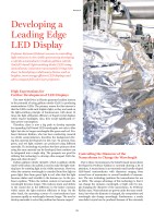
The 2014 Nobel Prize in Physics generated sudden interest in the potential of using gallium nitride (GaN) in producing semiconductor LEDs. The primary reason for this interest is that the LEDs would emit brighter light, as they are based on the light-emitting principle of luminescence with about 10 times the light utilization efficiency of liquid crystal displays which require backlights. Also, they would significantly re-duce power consumption.Therefore, there is now a big push to develop materials for expanding GaN-based LED wavelengths not only to blue light, but also to longer wavelengths like green and red. Pro-fessor Katsumi Kishino, who has been conducting research on nitride semiconductors, describes the background driv-ing this material development in this way: “At present, blue, green, and red light emitters are produced using different materials. If a technology to produce the three primary colors using the same material can be developed, these emitters can be integrated into a single chip. The prospects are good for utilizing this technology to develop ultra-compact LED dis-plays and other devices.”Indium gallium nitride (InGaN), which is gallium nitride (GaN) with indium (In) added, is used to make the light-emit-ting layer for emitting light in the visible spectrum. However, when the emission wavelength is extended from blue light to green light, then from green light to red, after that the light becomes darker and invisible to the human eye. As the pro-fessor explains, “When the indium content is increased, the wavelength becomes longer. This induces strain and defects in the crystal due to the difference in the lattice constant, which causes the light emission efficiency to drop. On the other hand, the operating current of a semiconductor laser increases rapidly as wavelengths become longer. The need to develop materials to solve this problem has become urgent.”High Expectations for Further Development of LED DisplaysDue to these circumstances, the InGaN-based nanocolumn developed by Professor Kishino is currently drawing a lot of attention. A nanocolumn is an extremely small needle-shaped GaN-based semiconductor with diameters ranging from several tens of nanometers to several hundreds of nanome-ters. The new technology positions the nanocolumns for use as LEDs. The unique advantage of this technology is that it can change the emission wavelength, or light color by sim-ply changing the diameter of the nanocolumn. As Professor Kishino says, “Nanocolumns are grown under the same condi-tions, but when the diameter is changed, the composition and wavelength also change accordingly. Furthermore, a nearly zero-defect crystal can be produced because of the extremely Controlling the Diameter of the Nanocolumn to Change the WavelengthDeveloping a Leading EdgeLED DisplayProfessor Katsumi Kishino’s success in controlling light emission in the visible spectrum by developing a nitride semiconductor (indium gallium nitride (InGaN)-based) light-emitting diode (LED) using nanocolumns (columnar nanocrystals) brings him closer to developing evolutionary devices such as brighter, more energy-efficient LED displays and ultra-compact full-color laser projectors.10Research
元のページ